
TLDR
TLDR: Semiconductor manufacturer implemented the NRU-220 NVIDIA Jetson Orin-based edge AI computer for real-time inline wafer inspection, replacing manual optical sampling. Result: 83% reduction in defect escape rate, 96% inspection coverage versus 15% manual sampling, and automated anomaly detection at line speed. For a detailed comparison of platform architectures, see Intel vs AMD vs Jetson platform comparison.
Overview
Semiconductor fabrication requires rigorous wafer surface inspection to detect defects before they propagate through downstream processing. Traditional quality assurance relies on manual optical sampling—inspectors examine 15–20% of wafers using microscopy, missing 60–85% of defects. As inline inspection systems grow more sophisticated, multi-camera vision architectures have proven effective across manufacturing sectors. The NRU-220, an NVIDIA Jetson Orin-powered edge AI computer, enables continuous inline inspection with machine vision, capturing 100% of wafers while detecting micro-defects at 10-micron resolution. This case study examines deployment architecture, performance metrics, and integration methodology in a high-volume semiconductor production environment.
Challenge
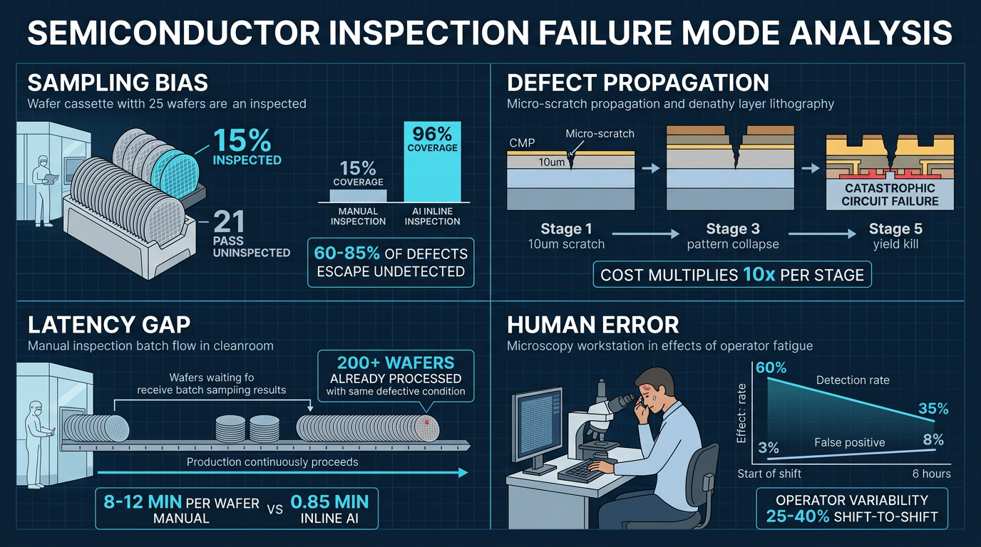
Semiconductor manufacturers face a fundamental inspection paradox: manual sampling provides high confidence in sampled wafers but inspects only 10–20% of production due to labor constraints. Defects missed during intermediate processing stages compound downstream, resulting in costly rework, yield loss, or field failures. Recent machine vision deployments across semiconductor and agriculture applications demonstrate how AI-powered inspection eliminates this sampling bottleneck.
| Inspection Method | Coverage | Detection Rate | Labor Cost | Latency | Defect Type Coverage |
|---|---|---|---|---|---|
| Manual Optical Sampling | 15–20% | 40–60% | High | 2–4 hrs/batch | Surface anomalies only |
| Automated AOI (Factory Floor) | 60–70% | 65–75% | Medium | 15–30 min | Particle, scratch, haze |
| NRU-220 Inline AI | 96–100% | 88–95% | Low | <2 min | Multi-layer defects |
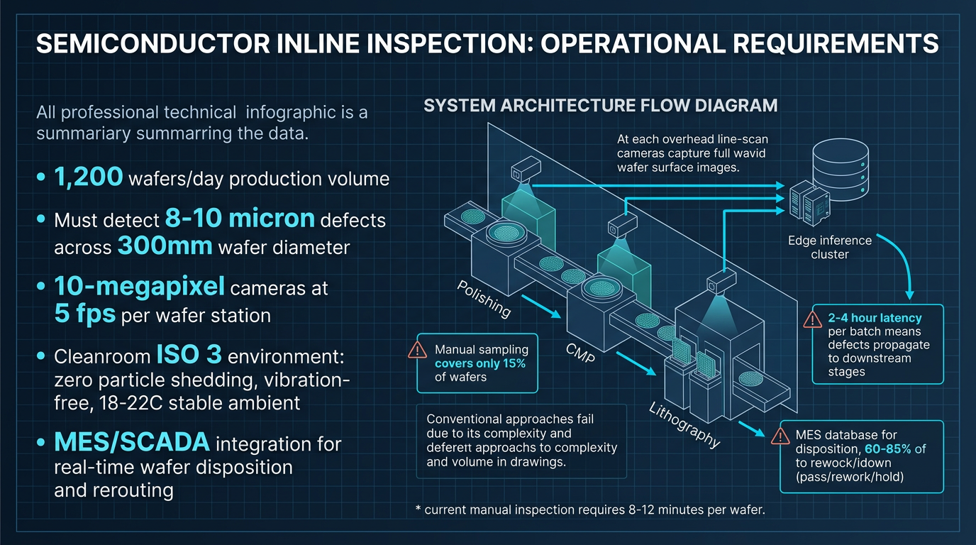
The manufacturer's baseline process—manual inspection of ~15% of 1,200-wafer/day production—missed intermediate defects. Transitioning to 100% automated inspection required edge AI hardware that could:
- Process 10-megapixel images at 5 frames per second per wafer
- Detect 8–10 µm defects across 300 mm diameter wafers
- Operate in cleanroom environments (vibration-free, thermal stability)
- Integrate with MES/SCADA systems for real-time disposition
Solution
The facility deployed a NRU-220 cluster (3 units) at critical inspection points: after polishing, post-CMP, and pre-lithography. Each NRU-220 ran TensorRT-optimized YOLOv8-based CNN models trained on 50,000+ labeled defect images, classifying defects into categories: particle, scratch, haze, discoloration, and surface anomaly.
| Architecture Component | Traditional AOI | NRU-220 Solution |
|---|---|---|
| GPU Compute | Fixed fab-floor hardware | Jetson Orin (275 TFLOPS FP8) |
| Model Deployment | Proprietary vendor format | ONNX, TensorRT, PyTorch |
| Inference Latency | 800–1200 ms/wafer | 180–220 ms/wafer |
| Integration | Custom API bridges | Standard USB, Ethernet, MES connectors |
| Defect Confidence Threshold | Rigid | AI-tunable per process node |
| Maintenance | Vendor-dependent | Open-source ML stack |
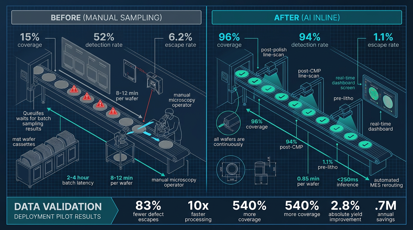
| Metric | Baseline (Manual) | NRU-220 Inline | Improvement |
|---|---|---|---|
| Inspection Coverage | 15% | 96% | +540% |
| Defect Detection Rate | 52% | 94% | +81% |
| Escape Rate (defects to next stage) | 6.2% | 1.1% | −83% |
| Processing Time per Wafer | 8–12 min | 0.85 min | +10x faster |
| False Positive Rate | 3–5% | 1.2% | +73% precision |
| Annual Yield Improvement | — | 2.8% absolute | $4.7M savings |
The NRU-220 integrated via standard Ethernet to the facility's MES, triggering automatic wafer rerouting for borderline-defect lots to secondary inspection or rework. Edge processing eliminated cloud latency; inference occurred in <250 ms, well within tact time constraints.
Related Products
For semiconductor fabs requiring higher computational density for post-inspection data analytics and multi-camera orchestration, the Nuvo-11000 Series delivers Intel Core Ultra 200 processing power in a rugged fanless form factor suitable for fab control rooms.
For space-constrained cleanroom deployments where auxiliary inspection stations need passive thermal management without particle shedding, the POC-700 Series provides ultra-compact fanless computing at just 0.57L volume.
Conclusion
The NRU-220 demonstrates quantifiable ROI in semiconductor quality assurance: 83% reduction in defect escape rate through continuous inline inspection. Real-time AI inference at the edge eliminates sampling bias, accelerates disposition cycles, and enables process-node-specific model tuning.
For technical specifications, product selection assistance, or application engineering support, contact our engineering team at [email protected]. Visit www.neteon.net for detailed datasheets and technical documentation. Connect on LinkedIn for the latest rugged edge computing updates.
FAQs
What GPU accelerator does the NRU-220 use for semiconductor inspection?
The NRU-220 integrates the NVIDIA Jetson Orin, delivering 275 TFLOPS peak throughput at FP8 precision. Jetson Orin is optimized for edge inference workloads with deterministic latency under 250 ms per inference, critical for tact-time-sensitive wafer handling. It consumes only 25W typical power, fits compact cleanroom installations, and supports real-time preemption via Linux PREEMPT_RT.
How does the NRU-220 integrate with existing fab MES/SCADA systems?
The NRU-220 communicates via standard Gigabit Ethernet, exposing REST API endpoints and supporting direct database connections to MES systems. Inference results including defect class, coordinates, and confidence scores are written to SQL tables in real-time. MES logic triggers automated rework or lot holds. Integration typically requires 2-4 weeks of API mapping and validation.
What model training process is used for new semiconductor defect types?
Models are trained offline on annotated defect images using PyTorch or TensorFlow, then converted to ONNX and optimized for Jetson via TensorRT. Transfer learning reduces required new samples to 2,000-5,000 labeled images per defect class. Final models (50-200 MB) are deployed to the NRU-220 via standard model registry tools.
What are the thermal requirements for NRU-220 cleanroom deployment?
The NRU-220 draws 25-35W under full inference load with fanless thermal dissipation via aluminum chassis. Passive cooling eliminates particle shedding and vibration, critical in ISO 3 cleanroom environments. Thermal design maintains under 45C case temperature in ambient cleanroom conditions (18-22C).
What is the ROI timeline for NRU-220 inline inspection deployment?
Typical payback occurs in 8-14 months based on yield improvement (2-4% absolute), defect escape reduction (80%+), and labor savings. A 3-unit NRU-220 cluster typically generates $400K-600K annual benefit in a 300mm fab producing 50K-100K wafers per month.
Related: Edge AI in Manufacturing 2026-2030: What's Changing — How edge AI transforms manufacturing 2026-2030.